


Product No: ESD-CDM
ESD-CDM is used for CDM electrostatic testing and is fully compliant with ANSI/ESDA/JEDEC JS-002-2014 “For Electrostatic Discharge Sensitivity Testing Charged Device Model (CDM) – Device Level”. The system is mainly composed of three parts: main instrument, DC high voltage source and electrostatic test probe (including attenuator). It can realize the electrostatic induction charging, electrostatic discharge and discharge signal acquisition test functions of the charged device model (CDM).
Specification:
DC high voltage source
a. Voltage output range: ±(10V~5kV);
b. Maximum allowable error of voltage output: ±(3%×reading value+10V);
Main instrument
a. Insulate the high-voltage induction plate to prevent high-voltage leakage;
b. The “high-voltage induction plate + isolation plate” can be adjusted in three directions, with an adjustment range of 0~10cm and an adjustment accuracy of 0.1mm (manual adjustment);
c. Sensor board size: 12cm*12cm*2mm;
d. Isolation board size: 12cm*12cm*0.4mm, material: FR4
Electrostatic test probe
a. Maximum measurement capability of electrostatic discharge current pulse peak ≥20A;
b. Probe size: Φ1.5*10mm, telescopic length: ≈3mm;
c. The test probe can move vertically (program control + manual control), with adjustable speed 0.1cm/s~5cm/s
d. The test probe part is equipped with an attenuator, and a data acquisition port/line is left for direct connection to an oscilloscope
e. Ground plane size: 63.5 mm*63.5 mm*6.35 mm
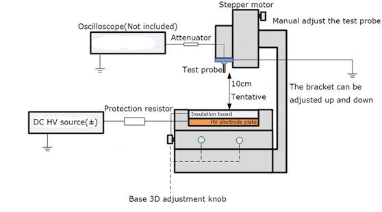
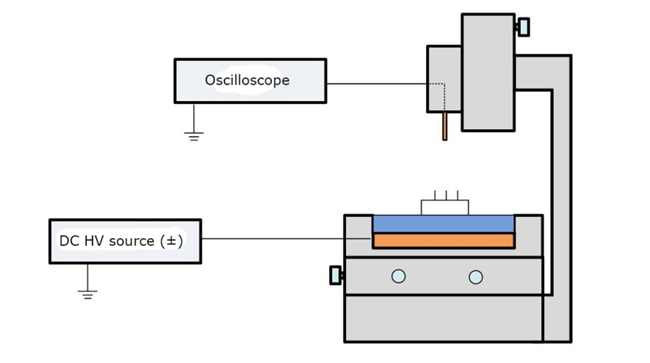
Schematic
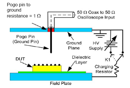
Principle reference diagram(ANSI/ESDA/JEDEC JS-002-2014)
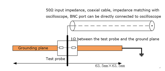
Schematic
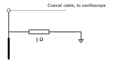
Equivalent circuit diagram
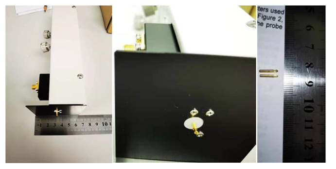
Test Probe Physical Reference Picture
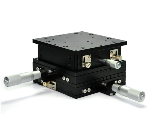
Base Physical Picture
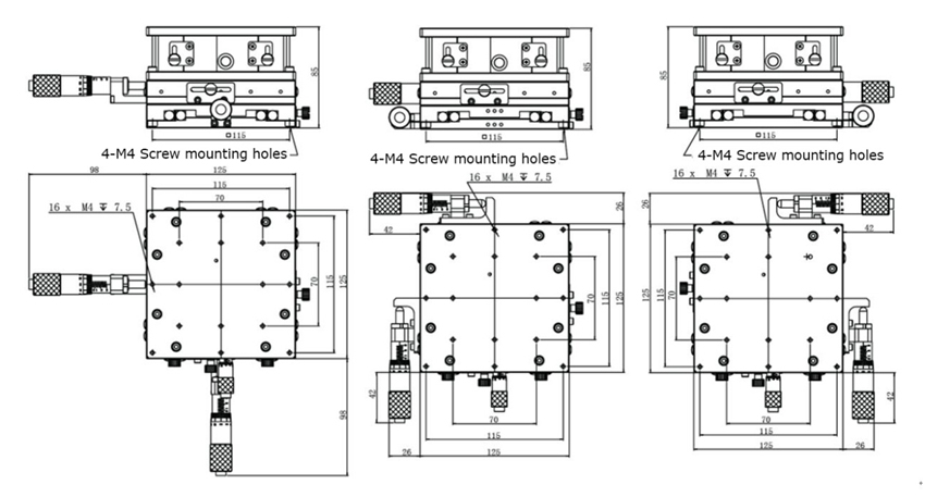
Schematic diagram of three-dimensional adjustment of the base (reference)
Test Operation Process:
1. Place the DUT on the insulation board, fix the fixture, and face the pin upward;
2. Manually adjust the three-dimensional knob of the base to make the pin of the DUT in the center;
3. Manually control the test probe to the maximum displacement, confirm that it is in contact with the pin, and then restore its position;
4. Set the probe movement speed to an appropriate value;
4. Start the high voltage source to XX volts to put the DUT in an electrostatically induced charged state;
5. Make the probe automatically move down quickly and contact the pin to complete the CDM discharge process. At the same time, the discharge waveform data is transmitted to the oscilloscope via a coaxial cable for display and storage.
Schematic Diagram Of The Test Operation Process

 中文简体
中文简体